Publications
Summary
While our research in the nano-design group spans a wide range of technologies moving forward, I have selected six publications here focusing on one specific emerging nanotechnology - carbon nanotubes - as a case study to illustrate the end-to-end technology development approach that we take in the nano-design group, all the way from low-level materials up to systems and applications. I also included figures from each publication as part of a whirlwind tour of this technological mini-journey:
Paper #1 provides motivation for why we should develop carbon nanotubes (CNTs) for energy-efficient digital VLSI - it can take years to develop a new technology, and so it is essential to ensure that the right technologies are being developed for the right applications. Then, paper #2 describes techniques to overcome major imperfections and variations associated with CNTs in order to realize their energy efficiency benefits. As experimental demonstration that these techniques work in practice, paper #3 describes a manufacturing methodology for CNTs that led to the most complex demonstration of any beyond-silicon emerging nanotechnology: a 16-bit microprocessor built entirely out of CNT field-effect transistors (CNFETs). Paper #4 shows that these technologies are now being transferred to high-volume commercial manufacturing facilities.
To achieve even larger energy efficiency benefits, paper #5 illustrates that CNFETs, like many emerging nanotechnologies, can be used to fabricate entirely new types of systems leveraging monolithic three-dimensional (3D) integration: with multiple layers of transistors and multiple layers of memory fabricated directly on top of each other, with ultra-dense and fine-grained vertical connectivity. Not only can these monolithic 3D systems overcome major bottlenecks associated with today's silicon-based digital VLSI systems (e.g., the memory wall), but also they can be used to enable entirely new types of systems and applications, e.g., with ultra-dense integration of sensors, computation, and memory, such as the monolithic 3D imaging system demonstrated in paper #6.
Below these selected publications, I included a more extensive list of publications by year (or check out my google scholar page). If these subjects are new to you, this magazine article can be a good place to start.
Selected Publications
Understanding Energy Efficiency Benefits of Carbon Nanotube Field-Effect Transistors for Digital VLSI
Gage Hills, Marie García-Bardón, Gerben Doornbos, Dmitry Yakimets, Pieter Schuddinck, Rogier Baert, Doyoung Jang, Luca Mattii, Syed Muhammed Yasser Sherazi, Dimitrios Rodopoulos, Romain Ritzenthaler, Chi-Shuen Lee, Aaron Von-Yew Thean, Iuliana Radu, Alessio Spessot, Peter Debacker, Francky Catthoor, Praveen Raghavan, Max Shulaker, H.-S. Philp Wong, and Subhasish Mitra
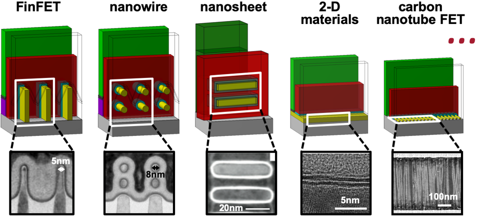
IEEE Transactions on Nanotechnology (TNANO), 2018Abstract - Carbon Nanotube Field-Effect Transistors (CNFETs) are highly promising to improve the energy efficiency of digital logic circuits. Here, we quantify the Very-Large-Scale Integrated (VLSI) circuit-level energy efficiency of CNFETs versus advanced technology options (ATOs) currently under consideration (e.g., silicon-germanium (SiGe) channels and progressing from today’s FinFETs to gate-all-around nanowires/nanosheets). We use industry-practice physical designs of digital VLSI processor cores in future technology nodes with millions of transistors (including effects from parasitics and interconnect wires) and technology parameters extracted from experimental data. Our analysis shows that CNFETs are projected to offer 9× energy-delay product (EDP) benefit (~3× faster while simultaneously consuming ~3× less energy) compared to Si/SiGe FinFET. The ATOs provide ≤50% EDP benefits. All analyses are performed at the same off-state leakage current density (≤100 nA per micron of FET width) and power density (≤100 W/cm2 of chip area). This analysis provides insights into the sources of CNFET EDP benefits and addresses key questions for deeply-scaled technologies. For instance, while contact resistance is a concern for sub-10 nm nodes, CNFETs still provide up to 6.0× EDP benefit (versus Si/SiGe FinFETs) using CNFET contact resistance values already experimentally achieved for 9 nm contact length.
Advanced Technology Options for Field-Effect Transistors (FETs). Collaborators: imec, TSMC. 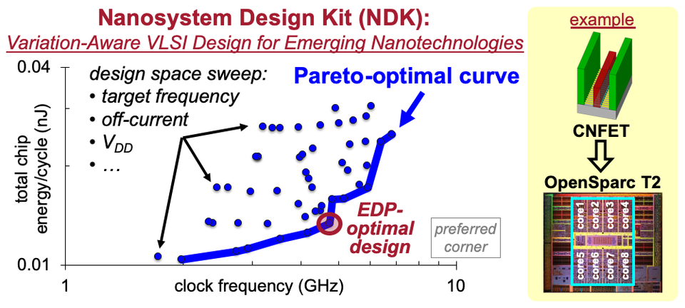
Nanosystem Design Kit (NDK) for designing and analyzing VLSI-scale circuits and systems using emerging nanotechnologies. Rapid Co-optimization of Processing and Circuit Design to Overcome Carbon Nanotube Variations
Gage Hills, Jie Zhang, Max Shulaker, Hai Wei, Chi-Shuen Lee, Arjun Balasingam, H.-S. Philip Wong, and Subhasish Mitra
IEEE Transactions on Computer-Aided Design of Integratd Circuits and Systems (TCAD) 2015Abstract - Carbon nanotube field-effect transistors (CNFETs) are promising candidates for building energy-efficient digital systems at highly scaled technology nodes. However, carbon nanotubes (CNTs) are inherently subject to variations that reduce circuit yield, increase susceptibility to noise, and severely degrade their anticipated energy and speed benefits. Joint exploration and optimization of CNT processing options and CNFET circuit design are required to overcome this outstanding challenge. Unfortunately, existing approaches for such exploration and optimization are computationally expensive, and mostly rely on trial-and-error-based ad hoc techniques. In this paper, we present a framework that quickly evaluates the impact of CNT variations on circuit delay and noise margin, and systematically explores the large space of CNT processing options to derive optimized CNT processing and CNFET circuit design guidelines. We demonstrate that our framework: 1) runs over 100× faster than existing approaches and 2) accurately identifies the most important CNT processing parameters, together with CNFET circuit design parameters (e.g., for CNFET sizing and standard cell layouts), to minimize the impact of CNT variations on CNFET circuit speed with ≤5% energy cost, while simultaneously meeting circuit-level noise margin and yield constraints.
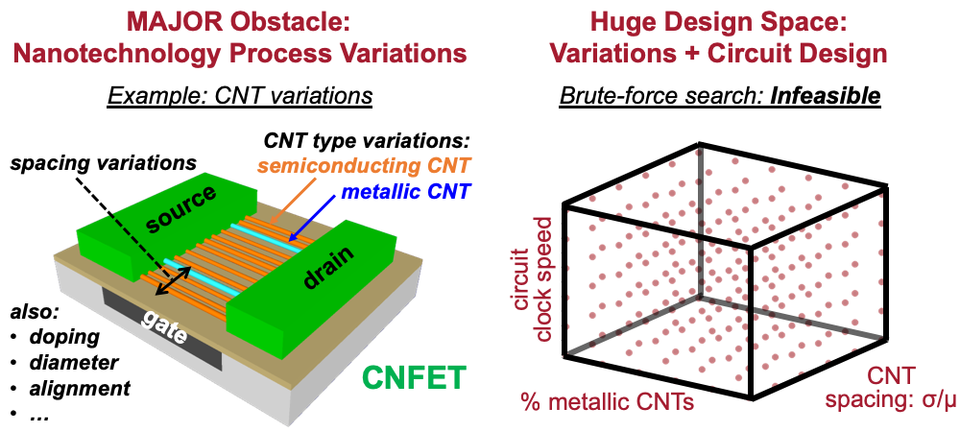
Major challenges associated with emerging nanotechnologies that must be overcome before nanotechnology benefits can be realized. 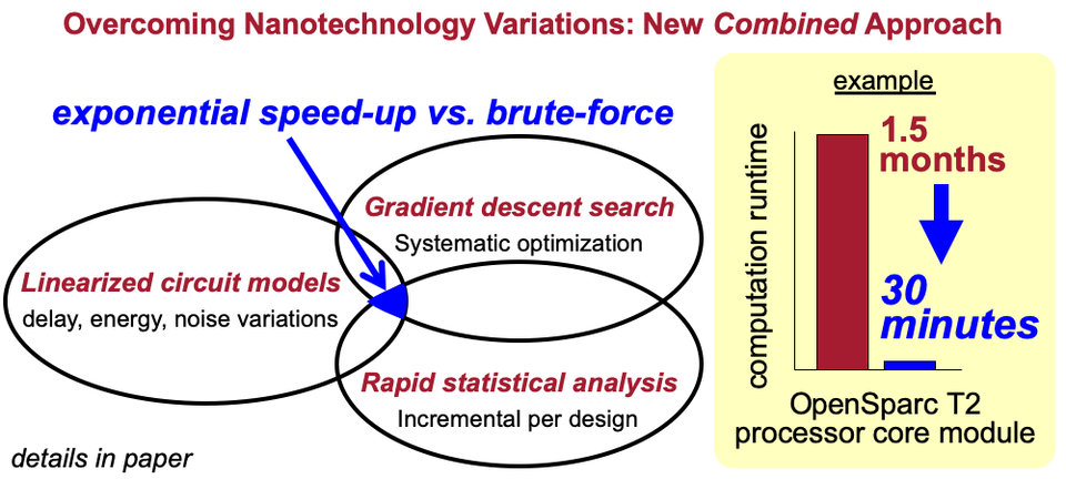
Rapid co-optimization of processing and circuit design to overcome nanotechnology variations. Modern Microprocessor built from Complementary Carbon Nanotube Transistors
Gage Hills & Christian Lau, Andrew Wright, Samuel Fuller, Mindy Bishop, Tathagata Srimani, Pritpal Kanhaiya, Rebecca Ho, Aya Amer, Yosi Stein, Denis Murphy, Arvind, Anantha Chandrakasan, and Max Shulaker
Nature, 2019Abstract - Electronics is approaching a major paradigm shift because silicon transistor scaling no longer yields historical energy-efficiency benefits, spurring research towards beyond-silicon nanotechnologies. In particular, carbon nanotube field-effect transistor (CNFET)-based digital circuits promise substantial energy-efficiency benefits, but the inability to perfectly control intrinsic nanoscale defects and variability in carbon nanotubes has precluded the realization of very-large-scale integrated systems. Here we overcome these challenges to demonstrate a beyond-silicon microprocessor built entirely from CNFETs. This 16-bit microprocessor is based on the RISC-V instruction set, runs standard 32-bit instructions on 16-bit data and addresses, comprises more than 14,000 complementary metal–oxide–semiconductor CNFETs and is designed and fabricated using industry-standard design flows and processes. We propose a manufacturing methodology for carbon nanotubes, a set of combined processing and design techniques for overcoming nanoscale imperfections at macroscopic scales across full wafer substrates. This work experimentally validates a promising path towards practical beyond-silicon electronic systems.

Beyond-Silicon microprocessor: RV16X-NANO, a 16-bit microprocessor built entirely out of carbon nanotube field-effect transitors (CNFETs). Heterogeneous Integration of BEOL Logic and Memory in a Commercial Foundry: Multi-Tier Complementary Carbon Nanotube Logic and Resistive RAM at a 130 nm node
T. Srimani & G. Hills, M. Bishop, C. Lau, P. Kanhaiya, R. Ho, A. Amer, M. Chao, A. Yu, A. Wright, A. Ratkovich, D. Aguilar, A. Bramer, C. Cecman, A. Chov, G. Clark, G. Michaelson, M. Johnson, K. Kelley, P. Manos, K. Mi, U. Suriono, S. Vuntangboon, H. Xue, J. Humes, S. Soares, B. Jones, S. Burack, Arvind, A. Chandrakasan, B. Ferguson, M. Nelson, M. M. Shulaker
MIT, SkyWater Technology Foundry, NanoIntegris, Intrinsix
VLSI, 2020Abstract - The inevitable slowing of two-dimensional scaling is motivating efforts to continue scaling along a new physical axis: the 3rd dimension. Here we report back-end-of-line (BEOL) integration of multi-tier logic and memory established within a commercial foundry. This is enabled by a low-temperature BEOL-compatible complementary carbon nanotube (CNT) field-effect transistor (CNFET) logic technology, alongside a BEOL-compatible Resistive RAM (RRAM) technology. All vertical layers are fabricated sequentially over the same starting substrate, using conventional BEOL nano-scale inter-layer vias (ILVs) as vertical interconnects (e.g., monolithic 3D integration, rather than chip-stacking and bonding). In addition, we develop the entire VLSI design infrastructure required for a foundry technology offering, including an industry-practice monolithic 3D process design kit (PDK) as well as a complete monolithic 3D standard cell library. The initial foundry process integrates 4 device tiers (2 tiers of complementary CNFET logic and 2 tiers of RRAM memory) with 15 metal layers at a ~130 nm technology node. We synthesize, fabricate, and experimentally validate the standard cell library across all monolithic 3D tiers, as well a range of sub-systems including memories (BEOL SRAM, 1T1R memory arrays) as well as logic (including the compute core of a 16-bit microprocessor) – all of which is fabricated in the foundry within the BEOL interconnect stack. All fabrication is VLSI-compatible and leverages existing silicon CMOS infrastructure, and the entire design flow is compatible with existing commercial electronic design automation tools.

The SkyTech Center at SkyWater Technology Foundry, where three-dimensional (3D) nanosystems leveraging CNFETs and Resistive Random-Access Memory (RRAM) are now being fabricated. 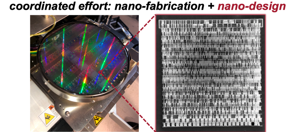
8 inch wafer fabricated at SkyWater, including RISC-V microprocessors built using CNFETs. Three-dimensional integration of nanotechnologies for computing and data storage on a single chip
Max M. Shulaker, Gage Hills, Rebecca S. Park, Roger T. Howe, Krishna Saraswat, H.-S. Philip Wong, and Subhasish Mitra
Nature, 2017Abstract - The computing demands of future data-intensive applications will greatly exceed the capabilities of current electronics, and are unlikely to be met by isolated improvements in transistors, data storage technologies or integrated circuit architectures alone. Instead, transformative nanosystems, which use new nanotechnologies to simultaneously realize improved devices and new integrated circuit architectures, are required. Here we present a prototype of such a transformative nanosystem. It consists of more than one million resistive random-access memory cells and more than two million carbon-nanotube field-effect transistors—promising new nanotechnologies for use in energy-efficient digital logic circuits[1,2,3] and for dense data storage[4]—fabricated on vertically stacked layers in a single chip. Unlike conventional integrated circuit architectures, the layered fabrication realizes a three-dimensional integrated circuit architecture with fine-grained and dense vertical connectivity between layers of computing, data storage, and input and output (in this instance, sensing). As a result, our nanosystem can capture massive amounts of data every second, store it directly on-chip, perform in situ processing of the captured data, and produce ‘highly processed’ information. As a working prototype, our nanosystem senses and classifies ambient gases. Furthermore, because the layers are fabricated on top of silicon logic circuitry, our nanosystem is compatible with existing infrastructure for silicon-based technologies. Such complex nano-electronic systems will be essential for future high-performance and highly energy-efficient electronic systems[5].
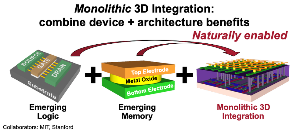
Monolithic three-dimensional (3D) integration - with multiple layers of logic and multiple layers of memory fabricted directly on top of each other with ultra-dense and fine-grained vertical connectivity - is enabled by emerging nanotechnologies that can be fabricated at low processing temperatures. 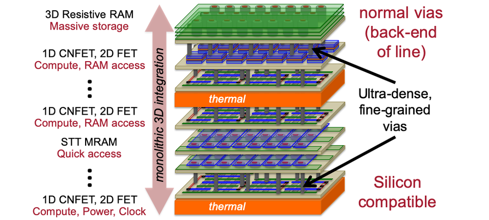
Example 3D nanosystem. 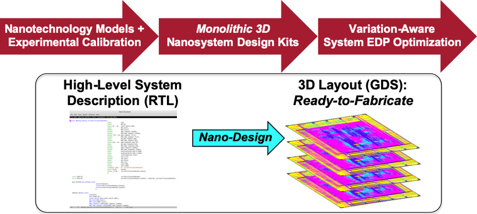
Nano-design design flow, from a high-level description of system (e.g., RTL = "Register Tranfer Level") to 3D layout (industry-standard GDS = "Graphic Database System" format) for final photomask generation. Monolithic Three-Dimensional Imaging System: Carbon Nanotube Computing Circuitry Integrated Directly Over Silicon Imager
Tathagata Srimani, Gage Hills, Christian Lau, and Max Shulaker
IEEE Symp. VLSI, 2019Abstract - Here we show a hardware prototype of a monolithic three-dimensional (3D) imaging system that integrates computing layers directly in the back-end-of-line (BEOL) of a conventional silicon imager. Such systems can transform imager output from raw pixel data to highly processed information. To realize our imager, we fabricate 3 vertical circuit layers directly on top of each other: a bottom layer of silicon pixels followed by two layers of CMOS carbon nanotube FETs (CNFETs) (comprising 2,784 CNFETs) that perform in-situ edge detection in real-time, before storing data in memory. This approach promises to enable image classification systems with improved processing latencies.
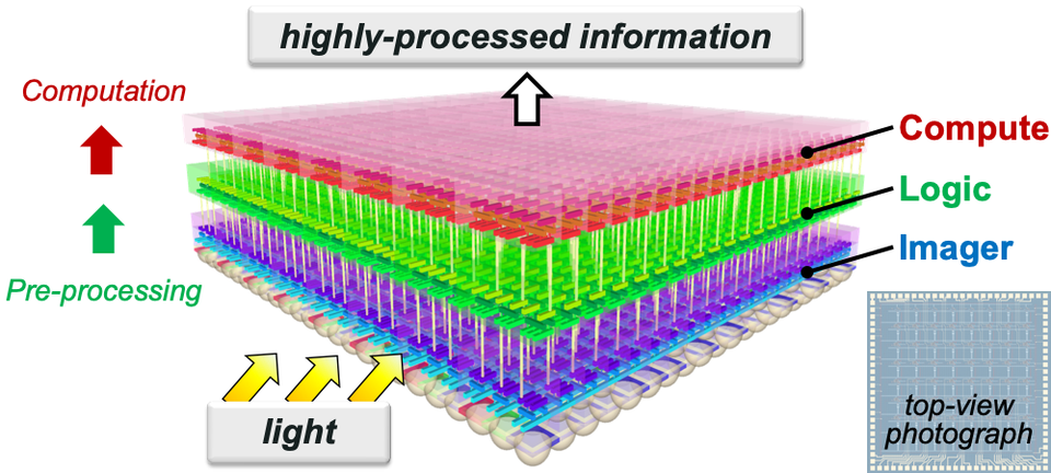
Monolithic 3D imaging system, with transitors (CNFETs) and memory (RRAM) fabricated directly on top of a silicon-based imaging pixel array, enabling camera systems to output highly processed information instead of raw pixel data.


Relevant Publications by Year
2020
T. Srimani & G. Hills, M. Bishop, C. Lau, P. Kanhaiya, R. Ho, A. Amer, M. Chao, A. Yu, A. Wright, A. Ratkovich, D. Aguilar, A. Bramer, C. Cecman, A. Chov, G. Clark, G. Michaelson, M. Johnson, K. Kelley, P. Manos, K. Mi, U. Suriono, S. Vuntangboon, H. Xue, J. Humes, S. Soares, B. Jones, S. Burack, Arvind, A. Chandrakasan, B. Ferguson, M. Nelson, M. M. Shulaker
MIT, SkyWater Technology Foundry, NanoIntegris, Intrinsix
VLSI SymposiumMindy D. Bishop, Gage Hills, Tathagata Srimani, Christian Lau, Denis Murphy, Samuel Fuller, Jefford Humes, Anthony Ratkovich, Mark Nelson, and Max M. Shulaker.
Nature ElectronicsManufacturing Methodology for Carbon Nanotube Electronics
Christian Lau, Gage Hills, Mindy D. Bishop, Tathagata Srimani, Rebecca Ho, Pritpal Kanhaiya, Andrew Yu, Aya Amer, Minghan Chao, and Max M. Shulaker
Invited Paper
VLSI Technology, Systems, and Applications (VLSI-TSA)Advances in Carbon Nanotube Technologies: From Transistors to a RISC-V Microprocessor
Gage Hills, Christian Lau, Tathagata Srimani, Mindy D. Bishop, Pritpal Kanhaiya, Rebecca Ho, Aya Amer, Max M. Shulaker
Invited Paper
International Symposium on Physical Design (ISPD)
2019
Modern Microprocessor built from Complementary Carbon Nanotube Transistors
Gage Hills & Christian Lau, Andrew Wright, Samuel Fuller, Mindy Bishop, Tathagata Srimani, Pritpal Kanhaiya, Rebecca Ho, Aya Amer, Yosi Stein, Denis Murphy, Arvind, Anantha Chandrakasan, and Max Shulaker
NatureCarbon Nanotube-based CMOS SRAM: 1 Kbit 6T SRAM Arrays and 10T SRAM Cells
Pritpal S. Kanhaiya, Christian Lau, Gage Hills, Mindy D. Bishop, Max M. Shulaker
IEEE Transactions on Electron Devices (TED)Asymmetric gating for reducing leakage current in carbon nanotube field-effect transistors
T. Srimani, G. Hills, X. Zhao, D. Antoniadis, J. A. del Alamo, and M. M. Shulaker
Applied Physics Letters (APL)Carbon Nanotube CMOS Analog Circuitry
Rebecca Ho, Christian Lau, Gage Hills, and Max Shulaker
IEEE Transactions on Nanotechnology (TNANO)
Best Paper AwardGregory Pitner, Gage Hills, Juan Pablo Llinas, Karl-Magnus Persson, Rebecca Park, Jeffrey Bokor, Subhasish Mitra, and H.-S. Philip Wong
Nano LettersTathagata Srimani, Gage Hills, Christian Lau, and Max Shulaker
IEEE Symposium on VLSI Technology1 Kbit 6T SRAM Arrays in Carbon Nanotube FET CMOS
Pritpal Kanhaiya, Christian Lau, Gage Hills, Mindy Bishop, and Max Shulaker
IEEE Symposium on VLSI TechnologySHARC: Self-Healing Analog with RRAM and CNFETs
Aya Amer, Rebecca Ho, Gage Hills, Anantha Chandrakasan, and Max Shulaker
IEEE International Solid-State Circuits ConferenceBeyond-Silicon Devices: Considerations for Circuits and Architectures
Gage Hills, H.-S. Philip Wong, Subhasish Mitra
Invited Book Chapter
Beyond-CMOS Technologies for Next Generation Computer Design
2018
Gage Hills, Marie García-Bardón, Gerben Doornbos, Dmitry Yakimets, Pieter Schuddinck, Rogier Baert, Doyoung Jang, Luca Mattii, Syed Muhammed Yasser Sherazi, Dimitrios Rodopoulos, Romain Ritzenthaler, Chi-Shuen Lee, Aaron Von-Yew Thean, Iuliana Radu, Alessio Spessot, Peter Debacker, Francky Catthoor, Praveen Raghavan, Max Shulaker, H.-S. Philp Wong, and Subhasish Mitra
IEEE Transactions on Nanotechnology (TNANO)Gage Hills, Daniel Bankman, Bert Moons, Lita Yang, Jake Hillard, Alex Kahng, Rebecca Park, Marian Verhelst, Boris Murmann, Max Shulaker, H.-S. Philip Wong, and Subhasish Mitra
Design Automation Conference (DAC)Energy-Efficient Digital VLSI Using Carbon Nanotube Field-Effect Transistors
Gage Hills
Ph.D. Dissertation, Stanford UniversityThe N3XT Approach to Energy-Efficient Abundant-Data Computing
Mohamed Sabry Aly, Tony Wu, Andrew Bartolo, Yash Malviya, William Hwang, Gage Hills, Igor Markov, Mary Wooters, Max Shulaker, H.-S. Philip Wong, and Subhasish Mitra
Proceedings of the IEEETony Wu, Haitong Li, Ping-Chen Huang, Abbas Rahimi, Gage Hills, Bryce Hodson, William Hwang, Jan Rabaey, H.-S. Philip Wong, Max Shulaker, and Subhasish Mitra
IEEE Journal of Solid-State Circuits (JSSC)30-nm Contacted Gate Pitch Back-Gate Carbon Nanotube FETs for Sub-3-nm Nodes
Tathagata Srimani, Gage Hills, Mindy Bishop, and Max Shulaker
IEEE Transactions on Nanotechnology (TNANO)Tunable n-Type Doping of Carbon Nanotubes through Engineered Atomic Layer Deposition of HfOX Films
Christian Lau, Tathagata Srimani, Mindy Bishop, Gage Hills, and Max Shulaker
IEEE Electron Device Letters (EDL)DISC-FETs: Dual Independent Stacked Channel Field-Effect Transistors
Pritpal Kanhaiya, Gage Hills, Dimitri Antoniadis, and Max Shulaker
IEEE Electron Device Letters (EDL)
2017
Three-dimensional integration of nanotechnologies for computing and data storage on a single chip
Max Shulaker, Gage Hills, Rebecca Park, Roger Howe, Krishna Saraswat, H.-S. Philip Wong, and Subhasish Mitra
NatureHysteresis-Free Carbon Nanotube Field-Effect Transistors
Rebecca Park, Gage Hills, Joon Sohn, Subhasish Mitra, Max Shulaker, and H.-S. Philip Wong
ACS NanoNegative Capacitance Carbon Nanotube FETs
Tathagata Srimani, Gage Hills, Mindy Bishop, Ujwal Radhakrishna, Ahmad Zubair, Rebecca Park, Yosi Stein, Tomás Palacios, Dimitri Antoniadis, and Max Shulaker
IEEE Electron Device Letters (EDL)
2016
Rebecca Sejung Park, Max Marcel Shulaker, Gage Hills, Luckshitha Suriyasena Liyanage, Seunghyun Lee, Alvin Tang, Subhasish Mitra, and H.-S. Philip Wong
ACS NanoTransforming nanodevices to next generation nanosystems
Max Marcel Shulaker, Gage Hills, H.-S. Philip Wong, Subhasish Mitra
Invited Paper
International Conference on Embedded Computer Systems: Architectures, Modeling, and Simulation (SAMOS)Time-based sensor interface circuits in CMOS and carbon nanotube technologies
Georges Gielen, Jelle Van Rethy, Jorge Marin, Max M. Shulaker, Gage Hills, H.-S. Philip Wong, Subhasish Mitra
Invited Paper
IEEE Transactions on Circuits and Systems
2015
Rapid Co-optimization of Processing and Circuit Design to Overcome Carbon Nanotube Variations
Gage Hills, Jie Zhang, Max Shulaker, Hai Wei, Chi-Shuen Lee, Arjun Balasingam, H.-S. Philip Wong, and Subhasish Mitra
IEEE Transactions on Computer-Aided Design of Integrated Circuits and Systems (TCAD)Efficient Metallic Carbon Nanotube Removal for Highly-Scaled Technologies
Max Shulaker, Gage Hills, Tony Wu, Zhenan Bao, H.-S. Philip Wong, and Subhasish Mitra
IEEE Proceedings of the International Electron Devices Meeting (IEDM)Energy-Efficient Abundant-Data Computing: The N3XT 1,000×
Invited Paper
IEEE Computer
2014
High-performance carbon nanotube field-effect transistors
Max Shulaker, Gregory Pitner, Gage Hills, Marta Giachino, H.-S. Philip Wong, and Subhasish Mitra
IEEE Proceedings of the International Electron Devices Meeting (IEDM)Sensor-to-digital interface built entirely with carbon nanotube FETs
Max Shulaker, Jelle Van Rethy, Gage Hills, Hai Wei, Hong-Yu Chen, Georges Gielen, H.-S. Philip Wong, and S. Mitra
Invited Paper
IEEE Journal of Solid State Circuits (JSSC)Robust design and experimental demonstrations of carbon nanotube digital circuits
Gage Hills, Max Shulaker, Hong-Yu Chen, H.-S. Philip Wong, and Subhasish Mitra
Invited Paper
IEEE Proceedings of the Custom Integrated Circuits Conference (CICC)
2013
Max Shulaker, Gage Hills, Nishant Patil, Hai Wei, Hong-Yu Chen, H.-S. Philip Wong, and Subhasish Mitra
NatureRapid Exploration of Processing and Design Guidelines to Overcome Carbon Nanotube Variations
Gage Hills, Jie Zhang, Charles Mackin, Max Shulaker, Hai Wei, H.-S. Philip Wong, and Subhasish Mitra
Design Automation Conference (DAC)
Best Paper Award nominationMax Shulaker, Jelle Van Rethy, Gage Hills, Hai Wei, Hong-Yu Chen, Georges Gielen, H.-S. Philip Wong, and Subhasish Mitra IEEE International Solid-State Circuits Conference (ISSCC)
Jack Raper Award for Outstanding Technology DirectionsSacha: The Stanford carbon nanotube controlled handshaking robot
Max Shulaker, Jelle Van Rethy, Gage Hills, Hong-Yu Chen, Georges Gielen, H.-S. Philip Wong, and Subhasish Mitra
Invited Paper
Design Automation Conference (DAC)Carbon Nanotube Circuits: Opportunities and Challenges
Hai Wei, Max Shulaker, Gage Hills, Hong-Yu Chen, Chi-Shuen Lee, Luckshitha Liyanage, Jie Zhang, H.-S. Philip Wong, and Subhasish Mitra
Invited Paper
Design, Automation, & Test in Europe (DATE)